Simultaneous measurements of electrical and mechanical properties
In the last 30 years, atomic force microscopy (AFM) has been extensively used to study materials and phenomena on a nanoscopic length scale. In particular, AFM’s ability to measure functional electrical properties like conductance or piezoelectric effects simultaneously with the topography has made AFM the analytical tool of choice for many fields such as semiconductors, sensors, or energy applications (e.g., solar cells). However, in standard contact mode, tip wear and damage to the surface still represent one of the main challenges, that limit reproducibility and cantilever lifetime.
To overcome these issues, Park Systems developed the PinPoint nanoelectrical modes that eliminate lateral shear forces between the cantilever tip and the surface, thus minimizing damage while ensuring high imaging quality and reproducibility for a wide range of samples over many consecutive measurements. In PinPoint mode, a force-distance curve is measured at each pixel, allowing a defined and safe physical contact between the tip and the surface. Decoupled XY- and Z- scanners enable a precise tip approach and retraction from the sample surface without lateral movement in X or Y direction during a force-distance curve, which effectively eliminates tip wear. Accordingly, this mode is especially useful for characterizing samples that are sensitive to shear force such as soft polymers, biological samples, or weakly adsorbed molecules. PinPoint can be combined with other AFM modes to obtain information about electrical properties such as:
- PinPoint Conductive AFM (C-AFM)
- PinPoint Piezoelectric Force Microscopy (PFM)
- PinPoint Scanning Spreading Resistance Microscopy (SSRM)
Also, a high-speed force-distance curve is simultaneously collected at each data point during PinPoint measurement. Therefore, this mode enables electrical characterization of samples in conjunction with their surface topography and mechanical properties at the same time (see “PinPoint nanomechanical mode note” for more details).

Figure 1. (a) Height image of F14H20 by Non-contact mode (b) Height image of F14H20 by Tapping mode (c) Line profile comparison
PinPoint C-AFM
Conductive AFM is a commonly used technique to characterize the current distribution (e.g., the local conductance) of various sample types such as insulators, semiconductors, and conductors. In C-AFM, a bias voltage is applied to the sample during scanning, and the current flow is measured by the tip. However, the current not only depends on the local sample properties but also on the contact force and tip geometry. Accordingly, changes in the tip geometry due to wear can alter the measured current and thus reduce the reproducibility and accuracy of the measurement.
In contrast, PinPoint C-AFM can provide a welldefined electrical contact between the AFM tip and the sample by precisely controlling the contact force and data acquisition time. Moreover, by eliminating lateral shear forces, PinPoint C-AFM allows for high spatial resolution imaging with high reproducibility.
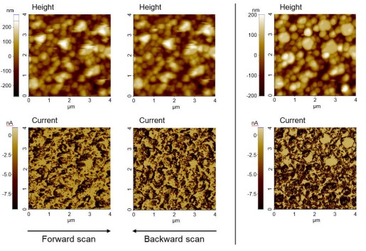
Figure 1 shows a comparison between conventional C-AFM and PinPoint C-AFM measurements on a vertically grown Zinc Oxide nanorods sample. Conventional C-AFM shows poor imaging quality as lateral forces cause damages to tip and sample, leading to reduced spatial resolution and imaging artifacts in height and current images. In contrast, PinPoint C-AFM mode produces sharp heightand current-images without artifacts, as presented in figure 1 (b).

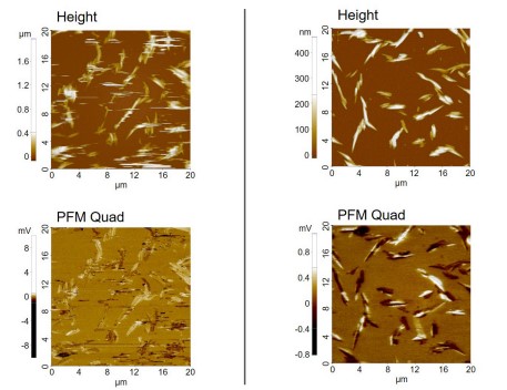
Figure 2. AFM height and PFM quad images obtained on annealed phenanthrene thin film using (a) conventional contact-based PFM and (b) PinPoint PFM. In (a), the phenanthrene is moved by the lateral force during contact scanning. This issue can be avoided when using PinPoint mode, as shown in (b).
PinPoint PFM
Piezoelectric Force Microscopy (PFM) allows measuring the electromechanical response of piezoelectric and ferroelectric materials when applying a bias voltage via the tip. Local piezoelectric domains in the sample expand or contract in response to the electric field between the tip and sample which is detected via the mechanical displacement of the cantilever. However, this displacement response sometimes is relatively small, which causes a small signal-to-noise ratio and difficult detection when using conventional PFM measurement. Since PinPoint PFM allows precise control of both the contact force and contact duration of the tip-sample interaction, measurement parameters can easily be optimized for high spatial resolution mapping of electromechanical properties. Figure 2 presents a comparison of conventional PFM and PinPoint PFM measurements on annealed phenanthrene thin film on an ITO surface. The rod-shaped nanostructures on the sample surface are susceptible to displacement during contact scanning, causing artifacts in AFM images, as shown in figure 2 (a). In contrast, PinPoint PFM shows improved height and PFM signals (figure 2 (b)).
PinPoint SSRM
Scanning Spreading Resistance Microscopy (SSRM) is well-known as a quantitative tool for studying current and resistance distributions of semiconductors. Typically, such materials are covered with thin films of surface contaminations or surface oxide layers, that impede the charge transport and thus hinder resistance distribution measurements. To counter that, typical AFM tips used for SSRM measurements are coated with hard materials like thin diamond films to scratch through the oxide/contamination layer to establish good electrical contact. Since high constant forces are needed to cut through the hard, insulating oxide layers, tip wear and surface defects in the conductive coating layer are typical issues associated with that measurement mode, leading to lateral resolution degradation and unstable electrical contact. These issues can be minimized using PinPoint mode. Accordingly, PinPoint SSRM provides accurate and reproducible data as demonstrated in figure 3. The resistance distribution of a lithium-ion battery electrode was studied while simultaneously imaging surface topography and mechanical properties at the same time, which deepens the understanding of electrical properties in conjunction with the surface and mechanical properties of a material.

Figure 3. (a) AFM height, (b) resistance, and (c) stiffness images obtained on a lithium-ion battery electrode using PinPoint SSRM mode. All three channels were acquired simultaneously in a single pass. Sample bias was set to +3 V. Measurement was conducted in vacuum using NX-Hivac system.
