The 13th edition of Graphene Conference series, the largest European Event in Graphene and 2D Materials, will be organized in Manchester, United Kingdom on June 27-30, 2023. Over the past editions, the Graphene Conference strengthened its position as the main in-person meeting point of the Graphene community Worldwide. Step by Park Systems booth to talk about advances in investigating 2D materials in nanorange!
We will be featuring Park Systems demo tools directly at our booth! Join us for live demonstrations on:
- • The FX40 Automatic AFM with innovative automation features, like inbuilt AI and machine learning, for nanoscale imaging
Don’t wait and book a demo slot today: pse.sales@parksystems.com
________________________________________________________________________________________________________

Join Dr. James Kerfoot, Application Scientist at Park Systems United Kingdom at GRAPHENE 2023 for his talk:
- ⏩ TALK: “Mapping tunnelling currents across switchable ferroelectric domains in parallel stacked layered materials with atomic force microscopy”
- ⏩ DATE: Thursday, June 29, at Workshop 8: Ferroelectrics & Piezoelectric 2DM
- [1] C. R. Woods et al. Nat Commun. 12, 347 (2021).
- [2] K. Yasuda et al. Science 372, 6549 1458 (2021)
- [3] M. Vizner Stern et al. Science 372, 6549, 1462, (2021)
- [4] Q. Zhao et al. J. Phys. Mater. 3 016001 (2020)
- [5] O. Kolosov et al. Phys. Rev. Lett. 74, 4309 (1995)
Abstract:
Presenting Author: James Kerfoot¹
Co-Author: Vladimir V. Korolkov¹
¹Park Systems UK Ltd, MediCity Nottingham, D6 Thane Rd, Nottingham, UK, NG90 6BH
pse@parksystems.com
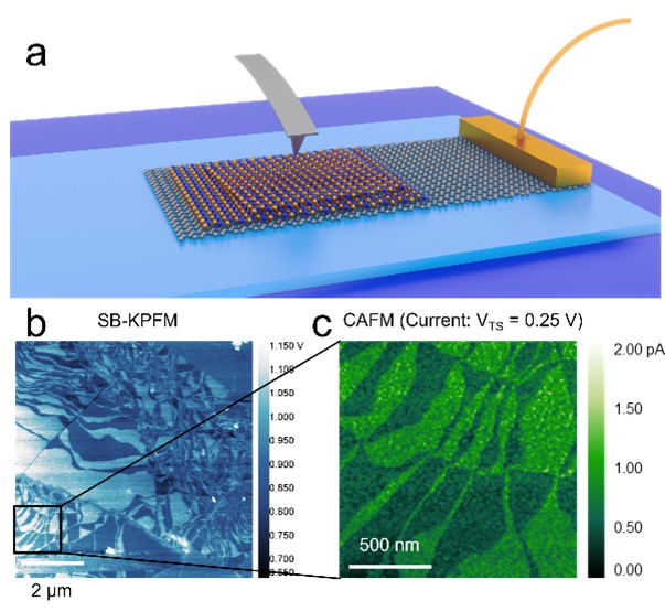
Controlling the twist angle between flakes of layered materials leads to interfacial ferroelectricity in the case of parallel stacked hexagonal boron nitride (hBN) [1-3]. We provide an account of the fabrication of such parallel stacked hBN samples using a home-built transfer setup [4] and the mapping of ferroelectric domains using various scanning probe techniques. We then discuss different ways in which such domains may be mapped and manipulated both electrically and mechanically [3,5]. We utilise conductive AFM (C-AFM) (where a tunnelling current is measured across a bilayer of parallel stacked hBN) to systematically study the variation of domain morphology versus mechanical setpoint and tip-sample bias. We show electrostatically induced switching of layer registry, enabling elevated relative areal coverage of AB domains versus BA domains depending upon the magnitude and direction of the applied bias. By performing C-AFM on parallel stacked hBN bilayers on graphene, we simultaneously map and manipulate the superlattice morphology to gain insights into both the mechanics of domain switching and tunnelling mechanisms under the influence of interfacial ferroelectricity. Such measurements are the nanoscale analogue of memristive tunnel diodes formed from parallel stacked hBN, which offer functionalities desirable for ‘more than Moore’ electronic devices.

Figure 1: Parallel stacked hBN may be formed by breaking and restacking exfoliated layers mechanically (a). Once formed, these structures may be characterised using KPFM to map the morphology of ferroelectric domains (b). For sufficiently thin layers (~0.6 nm), tunnelling current may be mapped using CAFM.
_______________________________________________________________________________________________________________________
About Graphene:
The Graphene Conference series, the largest European Event in Graphene and 2D Materials. Over the past editions, the Graphene Conference strengthened its position as the main meeting point of the Graphene community Worldwide.
